
@Earth Knowledge Bureau: China has started formulating the rules of the game, this time in the chip sector.
Just now, the Tao (τ) Law was officially released, marking the first time China has proposed a new principle to guide industrial development in the global semiconductor sector.
In fact, this law has been in practice within the industry for many years. This time, it is simply the first large-scale official announcement to the outside world, accompanied by a standalone theoretical framework.
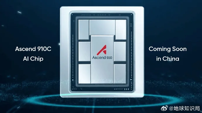
The core of the Tao Law is "logic folding technology," proposed by Huawei. Based on this law, 381 chips have been successfully designed and mass-produced over the past six years.
According to the current roadmap, by 2031, the transistor density of high-end chips based on this law will reach the equivalent level of the 1.4-nanometer process.
What is the definition of the Tao (τ) Law? And what is Tao (τ)? There is no need to worry about these, as they are too professionally technical; they are electrical engineering terms that the general public doesn't really need to understand.
If we summarize the Tao (τ) Law in plain language, it boils down to just eight words: "temporal scaling" replaces "geometric scaling."
Traditional chip manufacturing is like drawing on a fixed-size piece of paper where your pen can get increasingly finer—the process shrinks from 28nm, 14nm, and 7nm all the way down to 3nm and 2nm. By sharpening the pen tip, you can cram more transistors into the same area.
Why do it this way? Because "Moore's Law" is constrained by physical limits: when transistors shrink to 3nm, 2nm, and below, the quantum tunneling effect causes electrons to randomly "pass through walls" and leak, while the short-channel effect severely weakens the gate's control over the channel. As a result, the switching logic of 0s and 1s in transistors becomes unstable.
But the Tao (τ) Law takes a different approach: since the pen tip is already approaching the atomic level and hitting its limits, why not change the way we draw altogether?
By redesigning the internal transistor layout and signal transmission paths of chips through logic folding technology, signal propagation delay is continuously compressed. This increases transistor density without requiring the extreme etching of more advanced lithography machines.
This is also a new path that the Chinese semiconductor industry, under the constraint of being choked off from advanced processes, is attempting to forge by "using math to compensate for physics," stubbornly opening up a new route that does not rely on traditional geometric scaling.
It builds a multi-level collaborative optimization system that spans the device, circuit, chip, and system levels, with the goal of systematically reducing something called the "time constant" (Tao τ).
Beyond the Tao (τ) Law and Moore's Law, the semiconductor industry actually has a bunch of "unwritten rules."
For example, "Dennard Scaling," "Huang's Law," "Amdahl's Law," as well as the evolutionary trends of "More Moore" and "More than Moore" proposed by the industry.
In essence, these laws are techno-economic models; they are the "collective consensus" of industry participants at specific historical stages, rather than Newtonian physical laws.
If the Tao (τ) Law successfully plays out over the next five years, the way we talk about chips might really change—"how many nanometers" will no longer be the only benchmark. System-level innovation, full-stack software-hardware-chip collaborative design, and logic folding technology will become the new dimensions of competition.
Of course, a law is ultimately just a law, not magic.
Whether the Tao (τ) Law can become the next industry rule written into textbooks depends on whether the full-stack practice from devices to systems over the next six years can continuously deliver on its promises.
@PS3Paul: DeepSeek answers that the proposal of the "Tao Law" primarily holds the following four levels of significance:
1. Breaking physical limits: No longer relying on the traditional path of "making transistors smaller" (Moore's Law is approaching the atomic scale), but instead improving performance by compressing signal delay and optimizing logic structure, providing a viable "lane-change" solution for the post-Moore era.
2. Bypassing process blockades: Achieving transistor density equivalent to 1.4nm through design innovation helps reduce dependence on extreme manufacturing processes like EUV lithography. This holds strategic value for China's semiconductor industry, which is currently constrained by advanced processes.
3. Verifying engineering feasibility: Huawei has mass-produced 381 chips over 6 years and plans to implement "logic folding" technology in its autumn Kirin chips, indicating that the theory is not stuck in the conceptual phase but is a scalable engineering path.
4. Reshaping discourse power: This is the first time China has proposed an eponymous semiconductor development law at a top-tier global circuit conference, marking a shift from "following standards" to participating in and even leading the definition of industry roadmaps.
Indeed, the significance is profound
 微信扫一扫打赏
  支付宝扫一扫打赏
Comments (0)